Keynote Address & Guest of Honor Lectures
- PAVINARI Lecture Series on Women Physicists Delivered talk on ‘Tale of Photo 51 -Puzzle of DNA & Rosalind Franklin’ (May 2023)
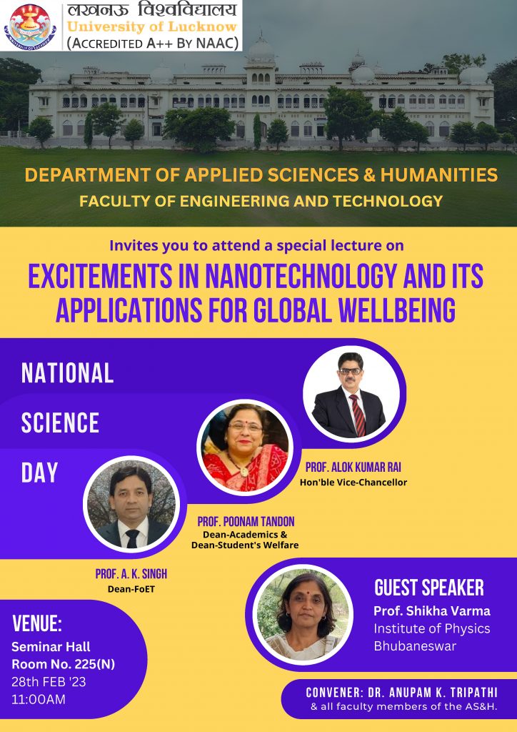
- Guest Speaker – Special Lecture on ‘Excitements in Nanotechnology and Its Applications for Global Wellbeing’ delivered on the occasion of ‘National Science Day-2023’ at Dept. of Applied Sciences & Humanities, Lucknow Univ., Lucknow (Feb. 2023)
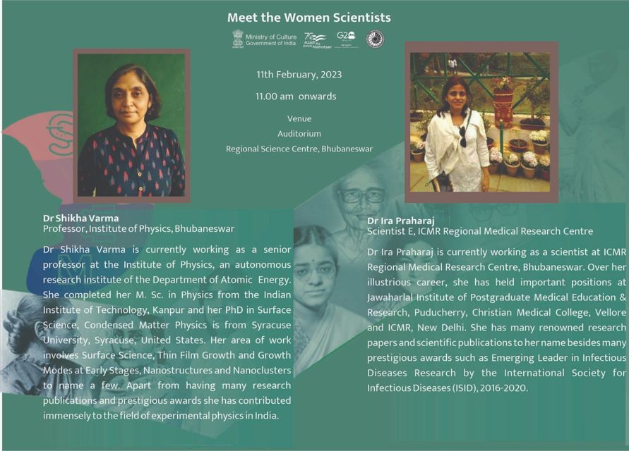
- Guest Speaker – Lecture on ‘Empowering the Women and Girls’ during Meet the Women Scientist program on the occasion of ‘International Day of Women & Girls in Science-2023’ organized by Regional Science Center, Bhubaneswar (Feb. 2023)
- Guest Speaker – Lecture on ‘Fascinating Surfaces, Nanoscience, Materials and their Applications’ on the occasion of ‘National Science Day-2022’ at Berhampur Univ., Berhampur (Feb. 2022)
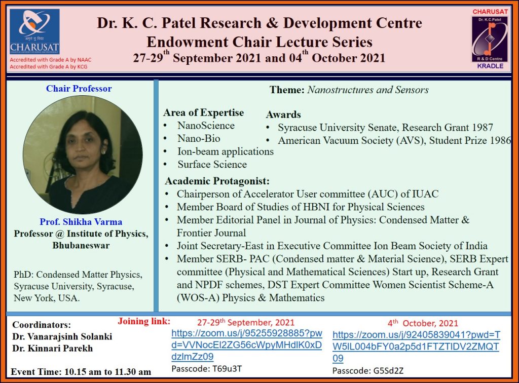
- Endowment Chair Lecture series on Nanostructure and Sensors at KRADLE, Charotar University of Science and Technology, Changa, Gujarat (Sept. and Oct. 2021)
- Career in Science : My Reflections at Virtual Lecture Series “Be The Change” At Isabella Thoburn College, Lucknow ( Oct 2020)
- Guest of Honor – Lecture on Excitements in Nanoscience delivered on the occasion of National Science Day-2020 at the Institute of Minerals and Materials Technology (IMMT), Bhubaneswar (Feb. 2020)
- Keynote Lecture DNA as a Programmable Sensor of Nanoparticles at the ‘Pressing for Progress 2019: Indian Physics Association (IPA) National Conference towards Gender Equity in Physics’ held at University of Hyderabad, Hyderabad (Sept. 2019).
Invited Talks, Colloquia, Seminars since joining IOP
- Invited Talk on Nanopatterning of Surfaces: For Sensors, Devices and Bio-applications at International Conference on Sustainable Nanomaterials Integration & Organization for Energy and Environment (iSNIOE2) 2024 (March 2024)
- Invited Talk on Designing Graphene Quantum dots and their Photo-response at Conference on Advanced Functional Materials and Devices – 2024 (AFMD), SRM, Nanotechnology Research center, SRM Institute of Science and Technology, Chennai (Feb. 2024)
- Invited Talk on Nanoscale patterning of Surfaces: For Sensors and Bio-applications at National Physicists’ Conclave 2024 (NPC 2024), SRM Institute of Science and Technology, Chennai (Feb. 2024)
- Invited Talk on Nanoscale Patterning of Surfaces: For Sensors and Bio-applications at Frontier Symposium in Physics-2024 (FSP 2024), IISER Thiruvananthapuram (Jan. 2024)
- Invited Talk on Nanopatterning of Surfaces: For Sensor, Device and Bio-applications at Meghnad Saha Memorial International Conference on Frontiers of Physics (MSMICFP-2023), University of Allahabad, Prayagraj (Nov. 2023)
- Invited Talk on Quantum Dots and Stone Wale Topological Defects in Graphene at International conference on Advanced Materials for Better Tomorrow (AMBT 2023), BHU, Varanasi (Oct. 2023)
- Invited Talk on Raman Spectroscopic investigations of Graphene Quantum Dots at National Workshop cum Hands-on Training Program on Raman Spectroscopy, NIT Rourkela, Rourkela (July 2023)
- Invited Talk on DNA and Organic Hybrid templates as Functional Materialsat 39th Annual convention of Orissa Physical Society (OPS) & National Seminar on Functional Materials For Emerging Technology (FMET-2023), at Silicon Institute of Technology, Bhubaneswar (Feb, 2023)
- Invited Talk on Quantum Dots and Stone Wale Topological Defects in Graphene at “PRL Conference on Condensed Matter Physics (CCMP-2023) at Physical Research laboratory (PRL), Ahmedabad (Feb. 2023).
- Invited talk on Characterizing Surfaces and Nanostructure: Investigations and Applications of Ion implanted Surfaces and NanoBio Hybrids at Pondicherry University, Poducherry ( Jan. 2023)
- Invited Talk on Functional Surfaces to Nanotechnology and “Nano Bio” given at “108th Indian Science Congress (ISC-2023)’’ held in Rashtrasant Tukadoji Maharaj (RTM) Nagpur Univ., Nagpur, (Jan. 2023).
- Invited Talk on ‘ Quantum Effects and Optical Studies of Nanostructure’ at Faculty Development Program on “Quantum transition from Ions to Cosmos (QTIC-2022)”, at Dept. of Phys., Odisha University of Technology and Research (OUTR), Bhubaneswar (Dec. 2022).
- Invited Talk on ‘ Applications with Functional Surfaces and Nanomaterials’ at Faculty Development Program on “Advancement in Materials Science and Nanotechnology” at Institute of Science, Shri Vaishnav Vidyapeeth Vishwavidyalaya, Indore (Nov.2022)
- Invited Talk on ‘Quantum dots and Topological defects in Graphene’ at 7th International Conference on Ion Beams in Materials Engineering and Characterization (IBMEC 2022) at Inter University Accelerator Center (IUAC), New Delhi, ( Nov. 2022)
- Invited talk on ‘DNA and Organic Hybrid templates as Functional Materials’at International Conference on Emergent Techniques and Functional Materials (ICETFM-2022) Medi-Caps University, Indore (July, 2022)
- Invited talk on ‘Characterizing Surfaces and Nanostructure: Morphology and Composition’ at High-End Workshop on “Scattering Methods (Electron, X-ray and Ion) for Materials Characterization DST-SERB “Karyashala” at IIT- Bhubaneswar (June. 2022)
- Invited talk on ‘DNA as a Functional Material’ at National Conference on Functional Materials: Synthesis, Properties and Applications (NCFM2022) organized by Department of Physics, Aligarh Muslim University, Aligarh, India (Feb. 2022)
- Invited Talk on ‘Nanopatterning of Surfaces for Sensor, Device and Bio-applications’ at International Conference on Accelerated Particles in Physics (APP-2022) organised by Hyderabad University, Hyderabad (Jan. 2022)
- Endowment Chair Lecture on ‘From Surfaces to Nanotechnology to Nano Bio’ at Charotar University of Science and technology, Changa, Gujarat (Oct. 2021)
- Endowment Chair Lecture on ‘Fabricating Useful Surfaces and Nanostructures’ at Charotar University of Science and technology, Changa, Gujarat (Oct. 2021)
- Endowment Chair Lecture on ‘Investigating Surfaces and Nanostructure: Morphology and Composition’ at Charotar University of Science and technology, Changa, Gujarat (Oct. 2021)
- Endowment Chair Lecture on ‘Applications with Surfaces and Nanostructures: Sensors and Catalysis’ at Charotar University of Science and technology, Changa, Gujarat (Nov. 2021)
- Invited talk on ‘Influence of Ion Irradiation for Phase transformation, Resistive switching and biocompatibility effects in thin oxide films’ at National Conference on Low Dimensional Systems: Properties and Applications ( LDSPA-2021) organized by Institute of Technical Education and Research, SOA, Bhubaneswar (July 2021)
- Invited talk on ‘Phase Transition in Ion Irradiated TiO2 : Resistive Switching Behavior and DNA Biocompatibility’ at 6th International Conference on Nanoscience and Nanotechnology (ICONN-21) organized online by SRM Institute of Science and Technology, Chennai ( Feb. 2021)
- ‘From Surfaces to Nanotechnology to “Nano Bio”’ at New Horizons in Physics: Indian Physics Association at 50’ Series organized by Indian Physics association IPA (Dec. 2020) https://www.youtube.com/watch?v=Bm41me52t_g
- Invited talk on ‘Phase Transformation and Resistive switching phenomenon in Metal oxide films’ at the International conference on Ions Beams in Materials Engineering and Characterizations (IBMEC 2020), organized online by IUAC, New Delhi ( Dec. 2020)
- Invited talk on ‘Resistive Switching memory, Thermal Transport and DNA Biocompatibility for Ion irradiated Metal-Oxide and Graphene films‘ at Asia Pacific Microscopy Conference (APMC-12) at Hyderabad International Convention Center (HICC) (Feb. 2020)
- Invited talk on ’Phase Transition in Ion Irradiated TiO2: Resistive Switching Behaviour and DNA Biocompatibility’ in International Conference on Nanostructuring by Ion Beams ( ICNIB-2019) organized at IGCAR, Kalpakkam (Nov. 2019)
- Seminar on ‘Phosphonic Acid thin films for detection of Arsenic in Water‘, at University of Nebraska, Lincoln, USA (March 2019).
- Colloquium on DNA as a Sensor of Nanoparticles: Unzipping and Changing Persistence Length of DNA, at University of Nebraska, Lincoln, USA (March 2019).
- Lecture on X-ray Photoelectron Spectroscopy (XPS) at International School on ‘Ion Beams in Material Science`, organized by IUAC, New Delhi (Oct 2018).
- Invited talk on Ion Beam Modified Surfaces, Roughness, Scaling properties, Fractal properties, at International School on ‘Ion Beams in Material Science`, organized by IUAC, New Delhi (Oct 2018).
- Colloquium on Nanotechnology & Viewing Atoms and Nanostructures at Uday Nath College, Adaspur. (Sept. 2018)
- Invited talk on DNA as a Sensor of Nanoparticles: Unzipping and changing Persistence length of DNA at International Conference on Microscopy and XXXIX Annual Meeting of EMSI 2018, at Mayfair Lagoon, Bhubaneswar ( July 2018)
- Invited talk Atomic Force Microscopy for the Study of Surfaces, Nanostructures and DNA at pre-conference workshop of International Conference on Microscopy and XXXIX Annual Meeting of EMSI 2018, at IOP Bhubaneswar (July 2018)
- Invited Talk on DNA as a Sensor of Nanoparticles: Unzipping and changing Persistence Length of DNA at IISER Kolkata (March 2018)
- Invited talk on Photoabsorption, Magnetism and DNA Biocompatibility on Nanostructured TiO2 (110) at the Ninth Vidyasagar-Satyendranath Bose National workshop (SMCP-2018) at Vidyasagar University, Midnapore, West-Bengal (Jan. 2018).
- Invited talk on DNA as a Sensor of nanoparticles: Unzipping of DNA at the International workshop on Advanced Materials (IWAM-2017) at the National Institute of Science and Technology (NIST), in Berhampur (Dec. 2017)
- Invited talk on Enhanced Photoabsorption, Super-Paramagnetism and DNA Biocompatibility in ion implanted TiO2 (110) at Meeting on Emerging Trends in the Physics of Surfaces, Interfaces and Nanostructures (ET-PSIN) at Indian Association for the Cultivation of Science (IACS) and S. N. Bose National Center for Basic Sciences (SNBNCBS),Kolkata (Nov. 2017)
- Invited talk on Sensing of Nanoparticles with DNA at National Conference on Physics at Small Scales and Advanced Materials (PSAM) at the School of Physics, University of Hyderabad (Sept 2017).
- Invited talk on DNA Sensing of Nanoparticles by Scanning Probe Microscopy at International Conference on Electron Microscopy and Allied Techniques and XXXVIII Annual Meeting of the Electron Microscope Society of India (EMSI-2017), held at Mahabalipuram (July, 2017).
- Invited talk on Nanoscience and Nano-Biotechnology at the Refresher Course in Physical Sciences held at Utkal University, Bhubaneswar (Mar. 2017).
- Invited talk on DNA as a Sensor of Nanoparticles: Unzipping and changing Persistence Length of DNA at the International conference on Advances in Biological Systems and Materials Science in NanoWorld (ABSMSNW -2017) held at BHU, Varanasi (Feb 2017).
- Invited talk on Interaction of DNA with oxidised Silicon Nanostructures at the International conference on Smart Materials & Applications (ISMA-2016), held at SOA-ITER, Bhubaneswar (Dec 2016).
- Invited talk on Enhanced Photoabsorption and Super-Paramagnetism in Cobalt implanted TiO2 at the International conference on Ions Beams in Materials Engineering and Characterizations 2016 (IBMEC 2016), held at IUAC, New Delhi ( Sept 2016).
- Invited talk on Nanotechnology and Atomic Force Microscopy, at the Faculty Development Program in the department of Physics, held at The College of Engineering and Technology (CET), Bhubaneswar ( Sept 2016).
- Invited talk on Photo- absorption properties of nanostructures fabricated by atom beam sputtering & interaction of nanostructures with plasmid DNA, at the Workshop on Future Directions in Ion Beams in Materials Engineering and Characterizations, held at IUAC, New Delhi (Dec. 2015).
- Invited talk on Bandgap Tuning, Better Photoabsorption and DNA Biocompatibility on TiO2(110) surfaces at the 60th DAE Solid State Physics Symposium held at Amity Univ., New Delhi (Dec. 2015).
- Invited talk on Nanodot Patterned surfaces for Photocatalysis at an International Conference on Frontiers in Material Science and Technology- ICFMST-2015 at National Institute of Science and Technology, NIST Berhampur, (Dec. 2015)
- Colloquium on DNA as a sensor of Mercury Nanoparticles at Syracuse University, Syracuse (NY), USA (Dec. 2015).
- Invited talk on Tuning of Bandgap Parameters for Photo-Catalysis and Enhancement of Bio-compatibility on Ion Beam Patterned TiO2 at International Conference on Energy Materials and nanotechnology-EMN Photocatalysis-2015 Conference at Las Vegas, USA (Nov. 2015).
- Invited talk on Low Energy Ion Beams: TiO2 (110), Si (100), Tantalum Patterning, Photo absorption, DNA Interaction, KMC modelling at Low Energy Ion Beam Facility workshop at IUAC Delhi (Nov. 2015).
- Invited talk on Fabrication of Nanostructure on rutile TiO2(110) surfaces by Low Energy Ion Beams : Enhanced Photoabsorption & Improved DNA Interaction through improved Hydrophilicity at ‘Workshop on Interdisciplinary investigations of Ion Beam Interactions with Matter: From Fundamental Aspects to Nanotechnology and Hadron- biology’ organized by IFCPAR (India French Center for the Promotion of the Advanced Research) in Caen, France (May 2015).
- Invited talk on Studies of nanostructures created on TiO2(110) by Low Energy Ion Beam Sputtering Technique: Role of Oxygen Vacancy at Surface Characterization Workshop: XPS,AES,TOF-SIMS, Physics Department, IIT Kharagpur, Kharagpur (Apr. 2015).
- Invited talk on Observations of Bandgap Tunability and DNA Biocompatibility on nanostructured TiO2(110) surfaces at ‘DAE-BRNS National Conference on Current trends in Advanced Materials`, VECC, Kolkata (Nov 2014).
- Invited talk on X-ray photoelectron Spectroscopy at International School on ‘Ion Beams in Material Science`, organized by IUAC, New Delhi (Oct 2014).
- Invited talk on Nanostructures and Nano-Bio studies with Low Energy Ion Beams at ‘Frontiers in Nuclear, Elementary Particle and Condensed Matter Physics’ organized by JINR (Joint Institute For Nuclear Research)-India Forum at Dubna, Russia (Jun. 2014).
- Invited talk on Tuning Bandgap Parameters for Photocatalysis & Enhancing Bio-compatibility of TiO2 (110) Nanostructures at ‘Third International Conference on Physics at Surfaces and Interfaces (PSI)` organized by Electron Microscopy Society of India, EMSI, Puri (Feb. 2014).
- Invited talk on X-ray Photoelectron Spectroscopy in Elucidation of Chemical States at Theme meeting on ‘Recent Advances in Material Characterization by Surface Analytical Techniques’ organized by NCCCM, BARC, Hyderabad (Feb. 2014).
- Invited talk on Fabrication of Nanostructures on TiO2 (110) surfaces by Low Energy Ion beam Sputtering: Enhanced Visible-Photoabsorption and Hydrophilicity at Discussion meeting on ‘Low Energy Ion Scattering at Molecular Solids’ organized by IIT Madras Chennai (Jan. 2014).
- Invited talk on Oxide Semiconductors: Bandgap Engineering & Optical Properties at Interaction Meeting on ‘Photoemission’ organized by Raja Rammana Centre for Advanced Technology, RRCAT(Aug. 2013)
- Invited Talk on Plenty of Room at the Bottom: Nanotechnology today at ‘One Day seminars on Feynman’s Birthday’ organized at IOP Bhubaneswar (May. 2013).
- Invited talk on Nanodot Patterned Rutile TiO2(110) Surfaces for Photocatalysis at National Conference on ‘Nano-materials as catalysts’ organized by Dept. of Chemistry, ITER, S O A University, Bhubaneswar (Jan. 2013).
- Invited talk on Biomolecules as Functional Nanomaterials at Conference on Condensed Matter and Biological Systems (CCMB13) organized by Physics Department, Banaras Hindu University, Varanasi (Jan 2013)
- Invited talk on Bandgap Tailoring & Biocompatibility in TiO2(110) Surfaces via Low Energy Ion Beam at the International conference on Swift Heavy ions in Materials Engineering and Characterization (SHIMEC 2012) organized by Inter -University Accelerator Center (IUAC), New Delhi ( Oct 2012).
- Invited talk on Bandgap Engineering and Enhanced Absorbance from Nanodot Patterned Rutile TiO2 (110) Surfaces at IIT Madras, Chennai (Aug 2012).
- Invited talk on Bandgap Engineering, Enhanced UV-Vis Absorbance and Higher PL Emission from Ion Beam Modified and Nanodot Patterned Rutile TiO2(110) Surfaces at International Conference on Advances and Trends in Engineering Materials and their Applications (Tenth AES-ATEMA- 2012) organized in Montreal University, Montreal, Canada (June 2012).
- Invited talk on Investigations of Rutile TiO2 Nanodots Formed by Low energy Ion beam Sputtering at ‘National Workshop on New and Nanomaterials’ organized by Institute of Materials Science & Science and Technology Department, Govt. of Odisha, at Bhubaneswar (Jan 2012).
- Invited talk Interaction of DNA with Hg clusters: tiny Mercury Sensor at ‘workshop on Photoemission Studies of Advanced Materials (PSAM)’ organized at IOP Bhubaneswar (Dec 2011).
- Invited talk on X-ray photoelectron spectroscopy (XPS) and its Applications for Nanostructures, Biology, Pollution, at ‘workshop on Electron Microscopy (WEM)’ organized at IOP Bhubaneswar (Nov 2011).
- Invited talk on Enhanced Photo-absorption and Photoluminescence Properties of TiO2 via nanostructures created by Ion sputtering at ‘Nanostructures by Ion Beams’ organized by IUAC-Delhi at Allahabad (Oct 2011).
- Invited talk on Tiny Mercury Sensors using DNA at conference on ‘Advanced Functional Materials’ organized at IOP Bhubaneswar (July 2011).
- Invited talk on Can DNA be used as a Sensor at ‘National workshop on Advanced Materials and Technology (NWAMT)’ organized by ITER – Bhubaneswar (Apr 2011).
- Invited talk on Enhanced Photo-absorption and Photoluminescence Properties of TiO2 at ‘International Conference on ‘Ion Beam Induced Nanopatterning of materials (IINM)’ organized at IOP Bhubaneswar (Feb 2011).
- Invited Talk on Patterning of TiO2 Surfaces by Low Energy Ion Beams at Inter University Accelerator Center (IUAC) New Delhi (Aug 2010).
- Invited Talk on on DNA as a sensor of Hg Nanoparticles at Inter University Accelerator Center (IUAC) New Delhi (Aug 2010).
- Lecture on Utilizing Physics Tools In Biology at “Refresher’s Course for College Teachers” organized by Biotechnology Department Utkal University, Bhubaneswar (Feb 2010).
- Invited talk on DNA as a Sensor at ‘Functional materials and Future Direction’s organized by Physics Department Utkal University, Bhubaneswar (Mar 2009).
- Invited talk on RBS and Channeling studies on Si(100) at QIP winter School on Optoelectronic Materials held at IIT Kharagpur, Kharagpur, India (Jan 99′).
- Invited talk on Surface patterning with Ion Beams at 2nd conference on Physics Surfaces and Interface (PSI) at Puri, India (Feb-2009).
- Invited talk on Nanostructures in ZnO and InP at One day Seminar on ‘High Tech Materials’ organized by Institute of Materials Science, Bhubaneswar (Nov. 2008).
- Invited talk on Pattern Formation with low energy Ion Beams at 4th Vacuum and Surface Sciences Conference of Asia and Australia (VASSCAA-4) at Matsue, Japan (Oct 2008).
- Colloquium on Fabrication of nanopatterns on InP(111) semiconductor surfaces at workshop on currents trends in Science and Technology of Materials at Salipur College, Salipur (July-2008)
- Invited talk on Electronic Structure and Scaling Studies of Surfaces Patterned By keV Ion Irradiation at Seminar-cum-Workshop on ‘Materials Characterization and Surface Modification in Research and Industry using Ion Accelerators (MCIA)’ organized by IOP Bhubaneswar (Apr2008)
- Invited talk on Experimental Facilities, Nano-Bio and Soft Condensed Matter Programs at Institute of Physics Bhubaneswar at Indo-Us workshop on ‘Science and Technology at Nano Bio interface’ organized by IOP Bhubaneswar (Feb2008)
- Invited talk on InP Nano dots Formation after keV Ar ion irradiation at International Workshop on Mesoscopic and Macroscopic Materials (IWMNMM) organized by Institute of Material Science, Bhubaneswar (Jan2008).
- Invited talk on Nano Pattern fabrication on semiconductor surfaces by ion beam irradiation at 52 DAE Solid State Physics Symposium University of Mysore, Mysore (Dec 2007)
- Invited talk on Characteristic Behavior and Scaling Studies of Self Organized InP Nano-dots formed via keV and MeV irradiation at the international Conference on Ion Beam Analysis (IBA) at Hyderabad (Sept 2007).
- Invited talk on Fabrication of InP Nano-dots, Magnetic Nano-dots of FeCr and Nano-dots of ZnO at French Delegate’s Meet organized by IOP Bhubaneswar (Sept 2007)
- Invited talk on Fabrication of Nano-dots and nano bio program at Nano-Meet organized by IOP Bhubaneswar (Aug 2007)
- Invited talk on Fabrication and Scaling Studies of Nano dots formed on InP after keV ion Irradiation at Inter University Center (IUC) Indore (Jul 2007).
- Invited talk on Techniques of AFM in a Refresher Course for College Teachers at IOP (Jun-2007)
- Invited talk on Characterization with Scanning Probe Microscopy (SPM) and X-ray Photoelectron Spectroscopy (XPS) techniques at ‘National Workshop in Nuclear and Atomic Techniques based inter disciplinary Research’ organized by IUC-Kolkata at Kalyani University, Kalyani (Mar 2007).
- Invited talk on Patterning of InP surfaces via Ion Beam Irradiation at ‘The Annual Workshop on Mesoscopic and Nanoscopic Materials’ at Institute of Material Science (IMS), Bhubaneswar (Mar 2007).
- Invited talk on Scaling Studies of Nanodots formed on InP(111) surfaces by Ion beam Irradiation-Sputtering at ‘The International Conference on Advanced Nanomaterials ANM-07’ held at IIT Mumbai (Jan 2007).
- Invited talk on Fabricating Nano dots by ion beam Implantation and Ion beam Irradiation at Inter University Accelerator Center (IUAC) New Delhi(Oct 2006).
- Invited talk on Formation of Nano Dots on InP(111) Surfaces after MeV Ion Implantation at National Conference on Recent Advances in Material Science (RAMS-06)’ at The Department of Physics, Kurukshetra University, Kurukshetra, (Sep 2006).
- Invited Talk on X-ray Photoelectron Spectroscopy in a Refresher Course for College Teachers at IOP (Jun-2005)
- Invited Talk on Scaling studies of nanostructures created after MeV implantation at Nuclear Science Center (NSC) New Delhi (Mar-2006).
- Invited talk on Nanoscale Structure Formation on InP(111) Surfaces after MeV Implantations at Indo-German Workshop on Synthesis and Modification of Nanostructured Materials by Energetic ions at NSC New Delhi (Feb-2005).
- Invited talk on Nanostucture Formation on InP(111) Surfaces after MeV Implantations at International Symposium on Advanced Materials and Processing, ISAMAP2K4, at IIT Kharagpur (Dec-2004).
- Invited talk on Scanning Probe Microscopy at Workshop on “Ion Beams in Material Science”(Oct-2004)
- Colloquium on AFM studies on Ion Implanted Surfaces at Material Science Department, IIT Kharagpur, Kharagpur(Aug-2004)
- Lecture on XPS and AFM studies in Ion Beam Research at IOP in a Refresher Course for College Teachers (Jun-2004)
- Invited Talk Invited talk Studies using XPS and AFM after Surface Modifications with Low energy Accelerator at Workshop on “Research with Low Energy Accelerators” arranged by IUC Indore at IOP (Feb-2004)
- Invited talk on Study of Surface modifications after Low Energy Implantations at IUCDAE workshop on `Utilization of Energetic Ion Beams for Materials Research’ in IGCAR (Jul-2003)
- Invited talk on Damage and substitution anomalies for MeV Sb implantation in Si after high energy irradiation at 20th International Conference on Atomic Collisions in solids at Toshali Sands, Puri (Jan 2003).
- Invited talk on Surface modifications in Si(100) due to Sb implantation : AFM and Channeling Study at International Conf. on Physics at Surfaces and Interfaces at Puri (March 2002).
- Colloquium on X-Ray Photoelectron facility at IOP at Geochemistry Group, LGIT, OSUG, Université Joseph Fourier, Grenoble, France, ( Dec 2002).
- Invited talk Scanning Tunneling Microscopy at ” I wanna Know” Series at IOP Bhubaneswar (Sept 2002).
- Lectures on X-ray photoemission technique and its applications in surface science at Refresher’s course for college teachers at IOP Bhubaneswar ( June 2002).
- Lectures on RBS and Channeling techniques and their Applications at ‘Orientation program of the scientific staff’ at IOP Bhubaneswar (May 2002).
- Invited talk on Anomalous Behavior of Implanted Sb at Workshop on ‘Low energy Particle Accelerators and their applications’ at IOP, Bhubaneswar (April 2002)
- Seminar on Sb implantation in Si(100) and the effects of defect-dopant interactions at University of California, Santa Barbara (CA),USA (Aug, 2001).
- Seminar on Production of Nanostructures of Si by MeV ion implantation in Si(100) at IIT Kanpur , India (May, 2000)
- Invited talk on Photoemission studies of Hg thin films on Ag(100) by Synchrotron Radiation at Synchrotron Radiation School for Indus-I held at CAT Indore, India (Jan.
- Invited talk on Characterizing Formation of Nanostructures and Damage In MeV implanted Si(100) at a National Conference on Materials and Surface Science with Accelerators, IOP, Bhubaneshwar, India (Oct 99′).
- Invited talk on Nanostructure of Si in Sb implanted Si(100) at a workshop on Nanomaterials and Clusters, IOP, Bhubaneshwar, India (Mar 99′).
- Invited talk on RBS and Channeling studies on Si(100) at QIP winter School on Optoelectronic Materials held at IIT Kharagpur, Kharagpur, India (Jan 99′).
- Invited talk on Implications of Er implantation in Si(100) QIP winter School on Optoelectronic Materials held at IIT Kharagpur, Kharagpur, India (Jan 99′).
- Colloquium on Studies of nanomaterials by AFM and STM at IIT Kanpur, Kanpur, India (Sept 98′).
- Seminar on Damage studies of MeV implantation in Si (100) at Nuclear Science Center, Delhi, India (Apr 98′).
- Invited talk on Rutherford Backscattering and Channeling Techniques and Their application to Antimony implantation in Silicon at , Pune, India, at Workshop on Ion Beams in Materials Research, organized by Inter University Consortium, Indore(Feb 97′).
- Invited talk on Activities and Facilities at IOP at , Pune, India, at Workshop on Ion Beams in Materials Research, organized by Inter University Consortium, Indore (Feb 97′).
- Invited talk on Low Dimensional Systems at Agartala, Tripura, India at Discussion meeting on Condensed Matter Days, (Aug. 96′).
- Colloquium on Studies in Surface Physics using Atomic Force Microscope and Scanning Tunneling Microscope at Ravenshaw College, Cuttack, India (Apr 96′).
- Colloquium on Study of InAs nanostructures using STM at IUC, Indore, India (Mar 96′).
- Invited talk Scanning Tunneling Microscopy study of InAs epitaxy on GaAs(001) , Bhubaneswar, India at Discussion meeting on Condensed Matter Days, IOP (Aug. 95′).
- Invited talk Pelletron Facility at Institute of Physics Bhubaneswar at IOP, Bhubaneswar, India at workshop on Material research with the Ion Beams and X-ray facilities, organized by IUC Indore, (Jul 95′)
- Invited talk Coverage dependent studies of InP/GaAs Using AFM at IOP, Bhubaneswar, India at Discussion meeting on Material Surfaces and Interfaces, (Apr. 95′)
Seminars Given Before Joining IOPB
- Seminar on Scaling for Island Growth at University of California at Santa Barbara, California, USA. (Sept. 1994)
- Seminar on The Study of MgO surfaces by Photoelectron Diffraction at the University of California at Santa Barbara, California, USA. (Nov. 1993).
- Seminar on Comparative Structural study of Ni, Co,and Cu ultrathin films and sandwiches by quantitative Auger electron diffraction at American Physical Society Conference in Indianapolis, Indiana, USA. (Mar.1993).
- Seminar on Study of MgO Surfaces by Photoelectron Diffraction at University of Wisconsin- Milwaukee, (Feb.1993).
- Seminar on The Study Of Single Crystal Surfaces by Photoelectron Diffraction at Tata Institute of Fundamental Research, Bombay, India. (Dec. 1992).
- Seminar on Thermal Desorption Spectroscopy at Case Western Reserve University at Cleveland, Ohio, USA. (Nov. 1990).
- Seminar on The Deposition of Molybdenum from Mo(CO)6 at Protective Coatings: Processing and Characterization, TMS Northeast Regional Meeting sponsored by The Minerals, Metals and Materials Society, ASM International, American Vacuum Society and New Jersey Advanced Technology Center for Surface Engineered Materials and held in Hoboken, New Jersey, USA. (May 1989).
- Seminar on The Correlation between Strain and Electronic Structure in Monolayer Thick Films at Materials Science and Engineering Conference in Buffalo, New York, USA. (July 1988).
- Seminar on Structure Induced Electronic States For Hg Overlayers on Ag(100) at American Physical Society Conference in Las Vegas, Nevada, USA. (March 1986).
- Seminar on Photoemission and Energy Loss Studies of Halogens adsorption on Fe(100) at Syracuse University , New York. Sept (1985).
- Seminar on Characteristic Energy Loss Studies of Molecular Halogens adsorbed on Fe(100) at American Physical Society Conference in Baltimore, Maryland. (March 1985).
Popular Science Talks
- Exciting Functional Materials & Applications of Nanoscience at Indian Association of Nuclear Chemists and Allied Scientists-Eastern Regional Center (IANCAS- ERC) program on ‘Wonder Materials, Energy and Radiation’ at Rama Devi (RD) University, Bhubaneswar (July 2022)
- From Surfaces to Nanotechnology to “Nano Bio” at Vigyan Vidushi Program organized by Homi Bhabha Science Center ( HBSC) and TIFR ( July 2022)
- ‘Fascinating Surfaces, Nanoscience, Materials and their Applications’ at National Science Day at Berhampur Univ., Berhampur (28 Feb 2022)
- Fascinating Surfaces, Nanoscience, Materials and their Applications at National Science Day at Institute of Physics, Bhubaneswar (28 Feb 2020)
- Nanotechnology: Viewing Atoms and Nanostructures at Udaynath College of Science and Technology at Adaspur, Cuttack ( Sept. 2018)
- Surface Science with Scanning Probe Microscopes at Third World Organization of Women Scientists (TWOWS) at Bangalore (Nov-2005).
- Looking at Electrons at Orientation of High School Students at IOP Bhubaneswar (April 2002).
Lucknow University, Lucknow
28-Feb-2023