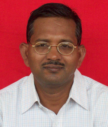
Parlapalli V. Satyam Professor |  |
| पिछले संगठन (चयनित) : |
- Ph.D. from Institute of Physics, Bhubaneswar, India
- Post doctoral fellow (Advanced Photon Source, Argonne National Lab., USA),
- JSPS Fellow (Japanese Science )
- Visiting Scientist (Nagoya University, Japan) - 2004, 2007
- Visiting Scientist (National Taiwan University, Taiwan) - 2008
- Visiting Scientist (NCKU, Tainan, Taiwan) - 2009
- Guest Scientist (University of Bremen, Bremen, Germany) - on Sabbatical leave since June 14, 2010 (for one year)
|
| कार्यग्रहण की तिथि :04/02/1999 |
| वर्किंग ग्रुप: : Experimental Condensed Matter Physics (Atomic Scale Physics at Surfaces and Interface |
| रुचि के क्षेत्र : |
Structural Studies from Low Dimensional System (Nanoscale), clean Surface and Interfaces, Experimental techniques associated with: Electron Microscopy (HRTEM, in-situ TEM, EELS (TEM), FEGSEM - FIB, MBE (UHV Growth), STM, X-Ray methods (XRD, XRR, XSW and using Synchrotron radiation), Ion Scattering methods and Ion implantation); Fundamental and Applied research in Nanoscience and Nanotechnology. |
| चयनित प्रकाशन : |
- Temperature dependent electron microscopy study of Au thin films on Si (100) with and without native oxide layer as barrier at the interface, A. K. Rath et al., J. of Physics D: Applied Physics (Accepted) (2011)
- Oxide mediated liquid-solid growth of high aspect ratio aligned gold silicide nanowires on Si (110) substrates, U. M. Bhatta et al., Nanotechnology 20 (2009) 465601
- Formation of aligned nanosilicide structures in a MBE-grown Au/Si(110) system: a real-time temperature-dependent TEM study, Bhatta et al., Journal of Physics: Condensed Matter 21 (2009) 205403
- Flux dependent MeV self-ion-induced effects on Au nanostructures: dramatic mass transport and nanosilicide formation, J. Ghatak et al., Nanotechnology 19 (2008) 325602
- Ion-beam-induced enhanced diffusion from gold thin films in silicon, J. Ghatak et al., Journal of Physics: Condensed Matter 20 (2008) 485008
|
| संपर्क : |
| कार्यालय : | R.N. 102,Extension Building 1 |
| ईमेल : | satyam@iopb.res.in |
| व्यक्तिगत होम पेज : | https://iopb.res.in/~satyam |

